

What is High Frequency PCB?
General Introduction of High Frequency PCB
High-frequency boards refer to special circuit boards with high electromagnetic frequencies, which are used for PCBs in the fields of high frequency (frequency greater than 300MHZ or wavelength less than 1 meter) and microwave (frequency greater than 3GHZ or wavelength less than 0.1 meters). The copper plate is a circuit board produced by using part of the process of the ordinary rigid circuit board manufacturing method or using a special treatment method. A high-frequency board can be defined as a circuit board with a frequency above 1GHz.
With the rapid development of science and technology, more
and more devices are designed for applications in the microwave frequency band
(>1GHZ) or even in the millimeter wave field (30GHZ), which means that the
frequency is getting higher and higher, and the demand for base materials is
also getting higher and higher, especially in the wireless networks. Satellite
communication is growing rapidly, information products are moving towards high
speed and high frequency. Therefore, developing new products always need to use
high frequency substrate, satellite system, mobile telephone receiving base
station and so on, these communication products must use high frequency PCB.
The Features of high frequency PCB
2. The DF should be small, which
3. The thermal expansion coefficient should be the same as
the copper foil as much as possible, because the difference will cause
4. The water absorption rate must be low. High water
absorption rate will affect DK and DF in a humid environment.
5. Heat resistance, chemical resistance, impact resistance
and peeling resistance must be good.
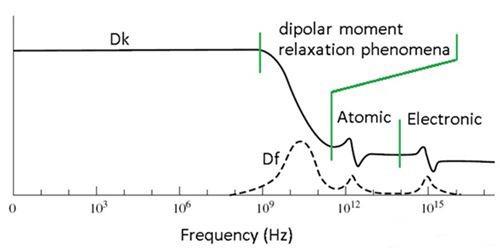
Materials for High Frequency Circuit Boards as shown in the picture below:
High frequency circuit board processing attention points:
1. The impedance control requirements are relatively strict, and the relative line width control is very strict, with a general tolerance of about 2%.
2. Due to the special plate, the adhesion of PTH copper sinking is not high. Usually, it is necessary to use plasma treatment equipment to roughen the vias and the surface to increase the adhesion of PTH hole copper and solder resist ink.
3. Do not grind the board before making the solder mask, otherwise the adhesion will be very poor, and it can only be roughened with micro-erosion potion.
4.Most of the plates are PTFE materials, and there will be many burrs when forming with ordinary milling cutters, so special milling cutters are required.
5.High-frequency circuit board is a special circuit board with high electromagnetic frequency.Generally speaking, high frequency can be defined as the frequency above 1GHz.
Its physical properties, precision, and technical
parameters are very demanding, and are often used in automotive anti-collision
systems, satellite systems, radio systems and other fields.
When we are producing high frequency circuit boards, we should pay attention to the following matters:
1. Reasonable selection of the number of layers: When
wiring high-frequency circuit boards, using the middle inner plane as the power
and ground layers can reduce parasitic inductance, shorten the length of signal
lines, and reduce cross-interference between signals.
2. Routing method: In PCB design, when routing
high-frequency circuit boards, the routing must be at a 45° angle, which can
reduce the transmission and mutual coupling of high-frequency signals.
3. The total length of the trace: In PCB design, the
shorter the total length of the trace, the better, and the shorter the parallel
spacing between the two wires, the better.
4. Number of vias: In PCB design, the fewer
5. The direction of the inter-layer traces: In the PCB (high
frequency circuit board) formulation, the direction of the inter-layer traces
should be vertical, that is, the top layer is in the horizontal direction, and
the bottom layer is in the vertical direction to reduce the influence of
signals on each other.
6. Copper plating: In the design of
7. Grounding: In the PCB design, when the high-frequency
circuit board is routed, the anti-interference ability of the signal can be
significantly improved by processing the grounding of the important signal
lines. Of course, the interference source can also be encapsulated to prevent
interference with other signals.
8. Power line: In the design of a high-frequency circuit
board (microwave radio frequency board), when the high-frequency circuit board
is routed, the signal traces cannot generate loops, and must be laid out in a
daisy chain.
9. Decoupling capacitor: In the design of a high frequency
circuit board (microwave RF board), when the high frequency circuit board is
routed, the decoupling capacitor is bridged at the power supply end of the
integrated circuit.
10. High frequency choke: In PCB design, when wiring the
high frequency circuit board (microwave radio frequency board), the high
frequency choke device needs to be connected when the digital ground wire and
the analog ground wire are connected, usually through the center
High Frequency PCB Manufacturing Capabilities
| No. | Category | High-Frequency PCB Capabilities |
| 1 | Material |
RO4003C, RO4350B, Ro3003, Ro3010, RT5880 |
| 2 | Number of Layers | 1-40 Layers |
| 3 |
Min. Track/Spacing |
2mil |
| 4 |
Min. Hole Size |
0.15mm |
| 5 |
Board Thickness |
0.3-3.1mm |
| 6 |
Finish Cooper |
0.6-12oz |
| 7 |
Silkscreen |
Green, Red, Yellow, White, Black, Blue, Purple |
| 8 |
Via Process |
Tenting Vias,Plugged Vias,Vias not covered |
| 9 |
Testing |
Fly Probe Testing (Free) and A.O.I. testing |
| 10 |
Surface Finishing |
HASL, HASL lead free, Immersion gold(ENIG), Immersion Tin, OSP, Immersion Silver(Ag) |
| 11 |
Solder Mask |
Green, Red, Yellow, White, Black, Blue, Purple |
| 12 |
Build Time |
8-11 days |
| 13 | Delivery Time | 3-4 days |
Choose AllWinPcba for your High Frequency PCB
AllWinPcba provides one-to-one service to better suit your need of high frequency PCB manufacturing. We welcome your inquiry about our high frequency PCB: svc@allwinpcba.com
High Frequency PCB Instant Quote
PCB Capabilities
PCBA Capabilities
SMD Stencil
Printed Circuit Boards
Product Show
Contact Us!
Our customer serviceready for your PCB
1.608.698.5398
SVC@allwinpcba.com