

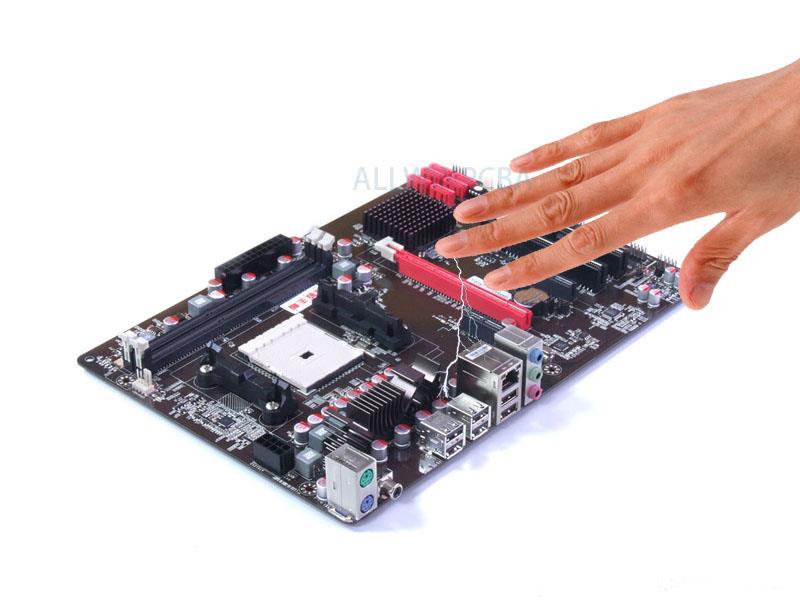
PCB Assembly Special Reminders
Parts Overages (It is for PCBA mass production.)
For the proper assembly of PCB during mass production, we require additional parts as overages; specifically, components such as resistors, capacitors and diodes. Components unused and in excess will be returned with your order.
Precautions for assembling components
1. Before assembly, the pins of electronic components should be wiped clean. It is best to wipe with a fine emery cloth to remove the oxide layer on the surface, so that it can be easily tinned when soldering. However, if the pins are coated, wipe as appropriate.
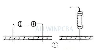
2. According to the assembly method of the components, vertical or horizontal assembly can be adopted, as shown in Figure 1. For components that can be assembled in two ways, when the working frequency is not too high, two assembly ways can be used; when the working frequency is high, the components should be assembled horizontally, and the leads should be as short as possible to prevent the influence of high-frequency parasitic capacitance circuit.
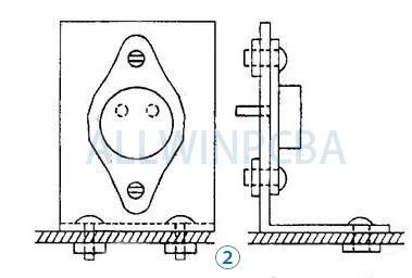
3. The suggestion of the PCB factory is that when assembling large and heavy components, in addition to soldering on the circuit board, it is best to use a bracket to fix it to make it more solid and reliable. FIG. 2 is a schematic diagram of the fixing method of the heavy component assembly bracket. In the figure, the high-power triode is fixed on the angle aluminum plate with screws, and then fixed on the assembly plate. In this way, one is stable, and the other is the aluminum plate that can play the role of heat dissipation.
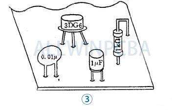
4. When assembling various electronic components, the side marked with the component model and value should face up or out, so that the component model data can be checked at a glance during soldering and maintenance, as shown in Figure 3.
5. When long component leads need to be retained, insulating conduits must be covered to prevent component pins from colliding and short-circuiting.
6. The assembly of components should be beautiful. When assembled vertically, the components should be perpendicular to the circuit board, and when assembled horizontally, they should be parallel to the circuit board of the PCB factory or attached to the circuit board.
The destructiveness of static electricity
1. Static electricity absorbs dust, changes the line impedance, and affects the function and life of components (principle: the mechanical effect of static electricity, so the surface of the PCB should be cleaned)
2. Heat generated by electrostatic discharge or current may cause potential damage to components
3. The high voltage of static electricity may break down the oxide film, causing interference or even damage to the components.
In order to prevent the damage of static electricity, the PCB should be packed in an anti-static shielding bag
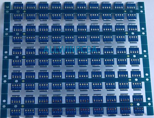
Panelization
1. The outer frame (clamping edge) of the PCB panel should adopt a closed-loop design to ensure that the PCB panel will not be deformed after being fixed on the fixture;
2. PCB panel width ≤260mm (SIEMENS line) or ≤300mm (FUJI line); if automatic dispensing is required, PCB panel width × length ≤125mm × 180 mm;
3. The shape of the PCB puzzle should be as close to a square as possible. It is recommended to use 2×2, 3×3,
4. The center distance between the small plates is controlled between 75 mm and 145 mm;
5. When setting the reference positioning point, usually leave a non-masked area 1.5 mm larger than the positioning point around the positioning point;
6. There should be no large components or protruding components near the connection point between the outer frame of the puzzle and the inner small board, and between the small board and the small board, and there should be a space greater than 0.5mm between the components and the edge of the PCB board. To ensure the normal operation of the cutting tool;
7. Open four positioning holes at the four corners of the outer frame of the jigsaw, with a diameter of 4mm±0.01mm; the strength of the holes should be moderate to ensure that it will not break during the process of upper and lower plates; the diameter and position accuracy should be high, and the hole wall should be smooth and free of burrs;
8. Each small board in the PCB puzzle must have at least three positioning holes, 3≤aperture≤6mm, and no wiring or patching is allowed within 1mm of the edge positioning hole;
9. The reference symbols used for the positioning of the entire PCB and the positioning of the fine-pitch devices. In principle, the QFP with a spacing of less than 0.65mm should be set at its diagonal position; the positioning reference symbols for the PCB sub-board should be set as For use, it is arranged at the opposite corner of the positioning element;
10. Large components should have positioning posts or positioning holes, such as I/O interfaces, microphones, battery interfaces, micro switches, headphone jacks, motors, etc.
environmental factor
Temperature, humidity and even G-forces are constantly acting on the PCB. If the materials and design specifications used are insufficient in size and ability to handle these conditions, the resulting board will always fail.
Choose AllWinPcba for your PCB Assembly requirement
AllWinPcba provides a one stop solution for all of your electronic manufacturing requirements with our experienced team and state-of-the-art assembly equipments under one roof in an inexpensive way, ranging from fast turnaround prototyping to high volume manufacturing. We have the capability to identify design and production issues during the prototype stage and solve these (in consultation with you) before mass production. Our turnkey or consigned printed circuit board assembly service is ISO ISO9001:2015-certified and RoHS compliant. We handle SMD, through-hole and mixed assembly projects. Look forward to cooperating with you, welcome your inquiry: svc@allwinpcba
PCB Assembly Online Quote
PCB Capabilities
PCBA Capabilities
SMD Stencil
Printed Circuit Boards
Product Show
Contact Us!
Our customer serviceready for your PCB
1.608.698.5398
SVC@allwinpcba.com