

PCB Assembly Process
General Introduction of PCB Assembly Process
In the component interconnection technology of electronic products, the most commonly used is the printed circuit board (PCB). With the ever-increasing packing density of modern electronic and mechanical components, the demand for printed circuit boards is increasing. As the number of layers on the printed circuit board increases, the printed lines become finer and the layers of the board become thinner. Especially in the past 10 years, as technology progresses, components get smaller and more difficult to assemble by hand and the number of components that may fit on a single board increase. Thus, the need for auto assembly was developed.
Although this article is elementary, it allows our customers to gain a bit of a better perspective on the process of the printed circuit board assembly.
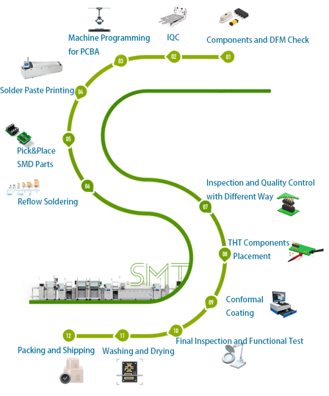
Step 1. Components and DFM Check
The PCB designer has prepared his layout on a Computer Aided Design or CAD system. Most PCB assembly companies need the design file of the PCB to start out, along with any other design notes and specific requirements. This is so the assembly company can check the PCB file for any issues that may affect the PCB's functionality or manufacturability. This is a design for manufacturability check, or DFM check, for short.
The DFM check looks at all the design specifications of a PCB. Specifically, this check looks for any missing, redundant or potentially problematic features. Any of these issues may severely and negatively influence the functionality of the final project. By identifying potential problems before manufacturing begins, DFM checks can cut manufacturing costs and eliminate unforeseen expenses. This is because these checks cut down on the number of scrapped boards. As part of our commitment to quality at a low cost, DFM checks come standard with every AllWinPcba project order.
Step 2. Incoming Quality Control (IQC)
AllWinPcba Verifying all incoming materials and handling quality problems before subsequent SMT assembly begins. Our IQC position will check following issues of incoming materials if they comply with our strict requirements. As follows:
1. model number and quantities according to BOM list.
2. shape (deformation, broken pin, oxidation etc), particularly for IC or other complex components.
3. sample test of incoming materials by tools such as test frame, multimeter etc.
4. If above defect or discrepancy occurs, we will return full incoming materials to supplier or customer.
Step 3. Machine programming for PCBA
Having received the PCB panels and components. This process is used by Process Engineers to program our Automatic Assembly Equipment (Printing, Pick and Place Machines, Soldering, AOI Inspection, X-Ray Machine). AllWinPcba has a proprietary, automated process that lets us set-up machines in hours. Gerber data is almost always available as this is the data required for the bare PCB to be manufactured.
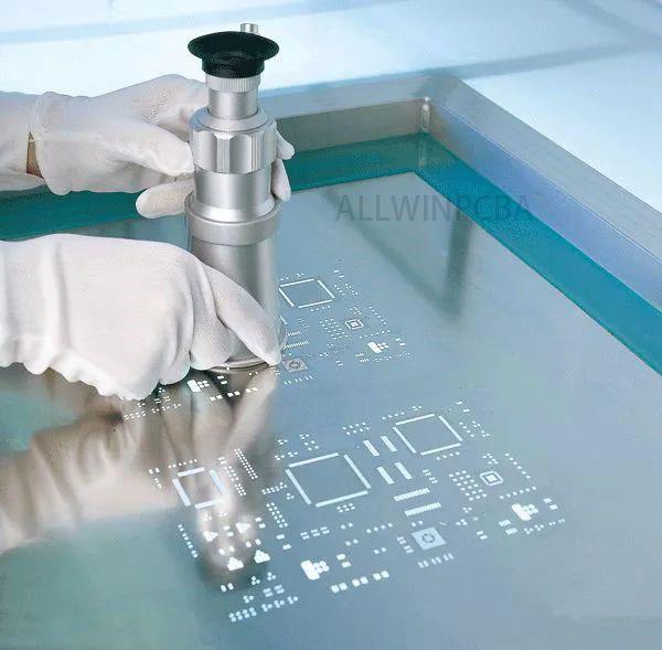
Step 4: Solder Paste printing
Solder paste printing is very important for PCBA, which directly affects the overall welding effect of PCBA. In the process of PCBA processing, how to do solder paste printing has become a problem that production managers must consider. The effect of solder paste printing is composed of four parts: steel mesh, solder paste, printing process and detection method. The following is a detailed analysis of Chang Kshun for you:
Solder PASTE IS printed ON PCB BOARD WITH steel mesh ON THE SOLDER pad OF ELECTRONIC component SMD to prepare FOR the welding of components. The equipment used is screen printing machine (printing machine), located in the front of the SMT SMT processing line.
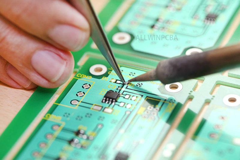
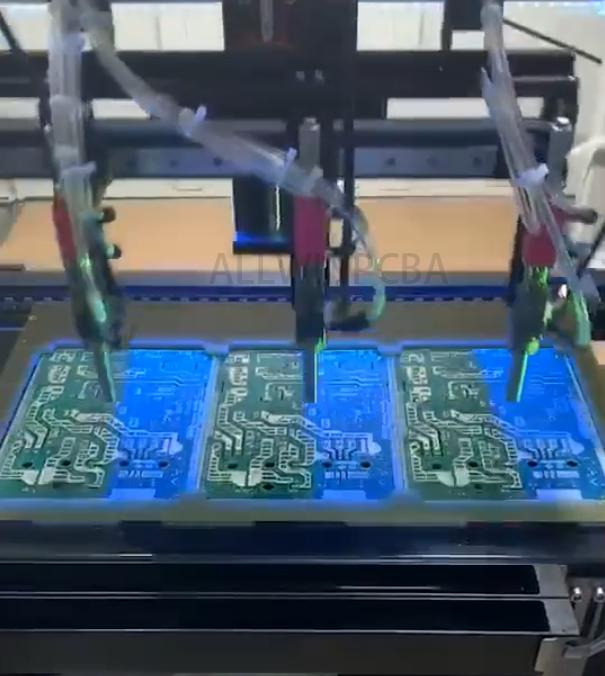
Step 5: Pick&Place SMD Parts
After applying the solder paste to the PCB board and passing the automatic inspection, the assembly process moves on to the pick and place machine (SMT Mounter).
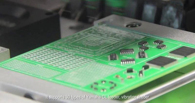
SMT machine is a core equipment in SMT production line, mainly used in electronic products source chip components mount. However, due to the different speed of the SMT machine and the different SMT products, the SMT machine is divided into high speed machine and Multi function machine
High speed machine: Used to attach the pin spacing is large, small components
Multi function machine: small pin spacing (pin density), large components.
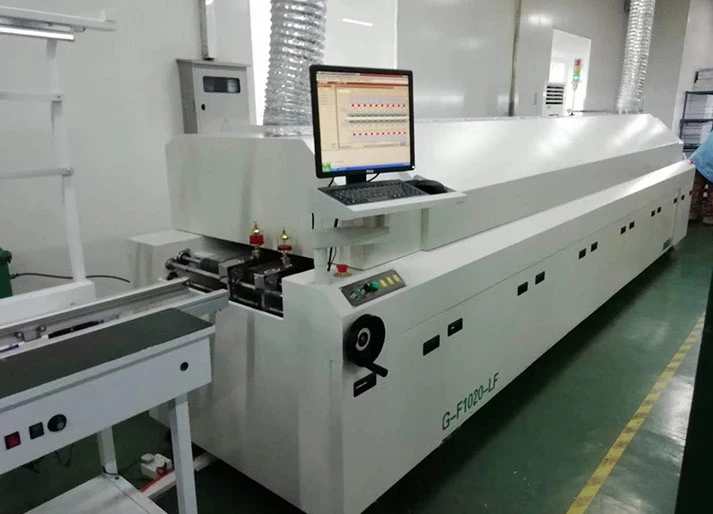
Step 6: Reflow Soldering
Once the components are placed on the boards, each piece is sent through our 10-zone reflow machines. This means the solder paste needs to solidify, adhering components to the board. PCB assembly accomplishes this through a process called "Reflow Soldering. "
The reflow soldering process is a surface mount board, it would appear to be one of the less complicated parts of the assembly processes, which can be divided into two types: single-sided mounting and double-sided mounting.
1. Single-sided mounting: pre-coating solder paste → patching (divided into manual mounting and automatic machine mounting) → reflow soldering → inspection and electrical testing.
2. Double-sided mounting: Pre-applied solder pastes on side A → SMT (divided into manual placement and automatic machine placement) → Reflow soldering → Pre-applied solder pastes on B side → SMD (divided into manual placement and automatic machine placement) placement) → reflow soldering → inspection and electrical testing.
The simple process of reflow soldering is "screen printing solder paste -- patch -- reflow soldering, the core of which is the accuracy of silk screen printing, and the yield rate of patch is determined by the PPM of the machine, and reflow soldering is to control the temperature rise and high temperature. and the falling temperature curve.”
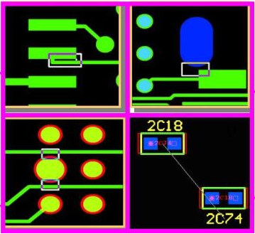
Step 7: Inspection and Quality Control with Different Ways
Once the surface mount components are soldered in place after the reflow process, the board can be checked whether the quality is acceptable. Often, movement during the reflow process will result in poor connection quality or a complete lack of a connection. Shorts are also a common side effect of this movement, as misplaced components can sometimes connect portions of the circuit that should not connect.
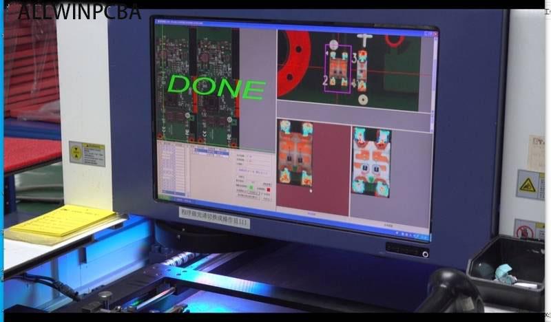
The most common of these inspection methods include the following:
1. Manual Checks: For smaller batches, that is, manually checking whether there are obvious defects in PCB appearance, solder pad, solder resistance ink, and outer line routing is simple and direct, but the efficiency is not high, and it is affected by the skill level of personnel.
2. Automatic Optical Inspection (AOI): AOI is a more appropriate inspection method for larger batches of PCBs. An AOI machine, uses a series of high-powered cameras to "see" PCBs. These cameras are arranged at different angles to view solder connections. Different quality solder connections reflect light in different ways, allowing the AOI to recognize a lower-quality solder.
3: Automated X-ray inspection (AXI): AXI is mainly used to detect the PCB inner line, mainly used in the high layer PCB circuit board test.
4. Flying Probe: It uses probes on the device to test from point to point on the circuit board (hence the name "flying needle") when ICT power is required. Since no custom fixture is required, it can be used for testing scenarios of PCB allegro and small and medium batch circuit boards.
5.aging test: Normally, the PCB is powered up and subjected to a limit aging test in the extreme harsh environment permitted by the design to see if it can meet the design requirements. Burn-in tests typically take 48 to 168 hours. But this test is not suitable for all use PCB, aging test will shorten the service life of PCB.
Anyhow, the fate of a malfunctioning board depends on the assembly company's standards. Malfunctioning boards are either sent back to be cleared and reworked, or they're scrapped. AllWinPcba's quality standards are based on the industry standard IPC-A-610 improved.
Step 8. THT Components Placement
Depending on the type of board under assembly, the board may include a variety of components beyond the usual SMDs. These include through hole technology (THT) components.
THT is a through-hole technology. THT is to plug components into the circuit board and then solder them firmly.
THT uses lead components. Circuit connection wires and mounting holes are designed on the printed board. The lead of the component is inserted into the through hole reserved on the PCB, and is temporarily fixed and welded on the other side of the substrate to form reliable solder joints and establish long-term mechanical and electrical connections.
Step 9: Conformal Coating
Some completed Printed Circuit Board Assemblies have a conformal coating. It's usually depends on the customer's product requirements.
Start by masking areas that do not need coating with tape, or use a temporary stencil to do this. The coating is then sprayed with a uniform thickness and allowed to dry. Once the PCBA is coated and dried, the battery pack can be installed and the final assembly completed.
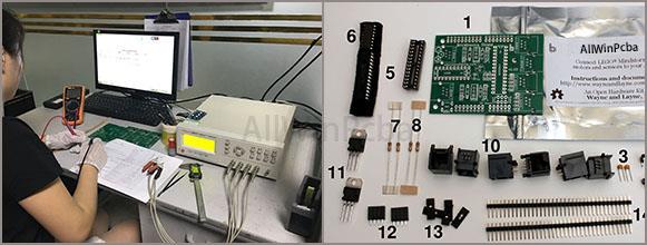
Step 10: Final Inspection and Functional Test
After the soldering and conformal coating step of the PCB assembly process is finished, a final inspection will test the PCB for its functionality by our Quality Assurance team. This inspection is known as a "functional test". The test software and tools are usually provided by the customer, AllWinPcba can also make fixtures according to customer requirements. The test puts the PCB through its paces, simulating the normal circumstances in which the PCB will operate. Power and simulated signals run through the PCB in this test while testers monitor the PCB's electrical characteristics.
If any of these characteristics, including voltage, current or signal output, show unacceptable fluctuation or hit peaks outside of a predetermined range, the PCB fails the test. The failed PCB can then be rework or scrapped, according to the industry standards or special standards for advance agreements with our customers.
Testing is the final and most important step in the board assembly process, as it determines the success or failure of the process. This testing is also the reason why regular testing and inspection throughout the assembly process is so important.
Step 11: Washing and Drying
AllWinPcba has a fully automated online cleaning machine, the cleaning machine for SMT/THT PCBA welding surface residual rosin flux, water soluble flux, non-cleaning flux/solder paste and other organic and inorganic pollutants for thorough and effective cleaning. It is suitable for large batch PCBA cleaning, using safe automatic cleaning equipment placed in DenSO production line, through different cavities online chemical cleaning (or water-based cleaning), water-based rinsing, drying all processes.
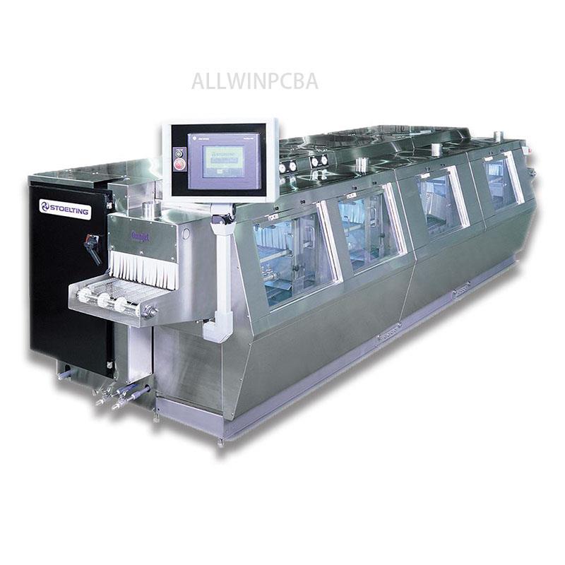
During the cleaning process, PCBA passes through the conveyor belt of the cleaning machine to clean the chamber in different solvents. The cleaning liquid must be compatible with components, PCB surface, metal coating, aluminum coating, label, handwriting and other materials. The special parts should be considered whether they can withstand cleaning.
The cleaning process is: into the plate → chemical pre-washing → chemical cleaning → chemical isolation → pre-rinsing → rinsing → spraying → air drying → drying
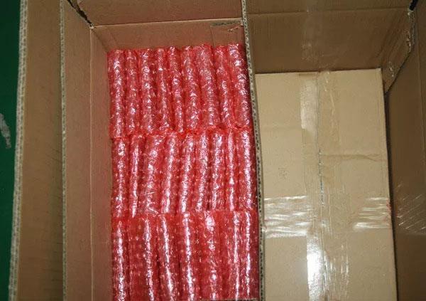
Step 12. Packing and Shipping
All assembled boards are packaged (can request in anti-static packaging) and shipped DHL, FedEx, UPS, and so on. Any unused components are returned in accordance with customer instructions. Additionally, customers are notified via email when their packages ships.
AllWinPcba provides a one stop solution for all of your electronic manufacturing requirements with our experienced team and state-of-the-art assembly equipments under one roof in an inexpensive way, ranging from fast turnaround prototyping to high volume manufacturing. We have the capability to identify design and production issues during the prototype stage and solve these (in consultation with you) before mass production. Our turnkey or consigned printed circuit board assembly service is ISO ISO9001:2015-certified and RoHS compliant. We handle SMD, through-hole and mixed assembly projects.
Choose AllWinPcba for your PCB Assembly requirement, welcome your inquiry: svc@allwinpcba.com
PCB Assembly Online Quote
PCB Capabilities
PCBA Capabilities
SMD Stencil
Printed Circuit Boards
Product Show
Contact Us!
Our customer serviceready for your PCB
1.608.698.5398
SVC@allwinpcba.com