


How to Avoid Common PCB Assembly Defects: A Complete Guide
 17 Aug 2026
By Jack Liu
17 Aug 2026
By Jack Liu
Introduction
For overseas OEM and ODM buyers, PCB assembly defects are not just factory problems. They become late shipments, unstable field performance, extra inspection cost, urgent engineering calls, and sometimes product launch delays. A small solder bridge can stop a smart home device from powering on. A reversed diode can fail a whole batch. Poor through-hole solder filling can pass visual inspection but fail after vibration in an industrial controller.
The expensive part is that many PCBA defects are preventable. Most failures come from incomplete design data, poor DFM review, unsuitable component packaging, weak process control, or rushed production approval. This guide explains the most common PCB assembly defects and how buyers, designers, and procurement teams can reduce them before mass production.
________________________________________
Why PCB Assembly Defects Happen
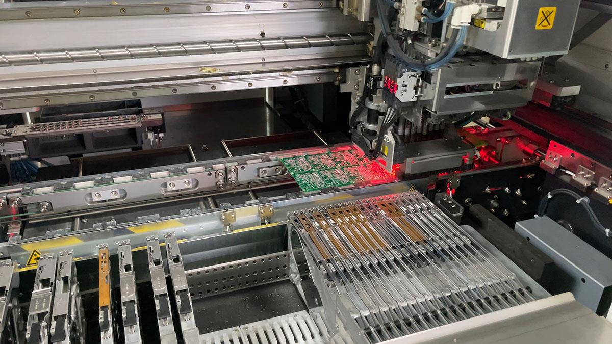
PCB assembly is a chain process. Gerber files, BOM accuracy, component quality, solder paste printing, SMT placement, reflow soldering, DIP insertion, inspection, cleaning, and testing all affect the final board.
A defect often appears at the production line, but its root cause may start earlier. Tombstoning may look like a soldering issue, but it may be caused by unbalanced pad design. A missing part may look like an operator mistake, but the real cause may be an unclear BOM or wrong feeder setup.
Procurement tip:
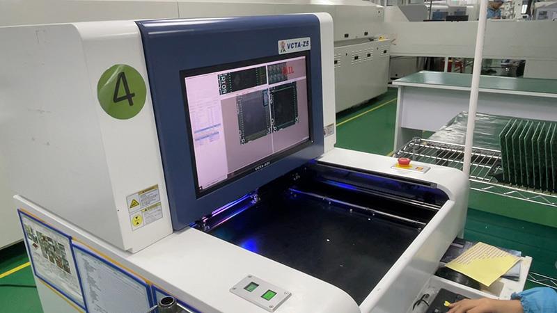
Before asking for the lowest PCBA manufacturing price, confirm whether your supplier performs DFM, DFA, first article inspection, AOI, X-ray when needed, and functional testing.
________________________________________
Common PCB Assembly Defects and How to Avoid Them
1. Solder Bridging
Solder bridging happens when excess solder connects two pads or pins that should remain separate. It is common on fine-pitch ICs, connectors, and dense SMT layouts.
Typical causes include too much solder paste, inaccurate stencil aperture design, poor solder mask clearance, component shift, or incorrect reflow profile. To prevent it, review pad spacing during DFM, optimize stencil thickness, reduce paste volume on fine-pitch pads, and use AOI after reflow.
2. Insufficient Solder
Insufficient solder means the joint does not have enough solder to create reliable electrical and mechanical connection. It may cause intermittent failure after vibration, thermal cycling, or long-term use.
Causes include blocked stencil apertures, low paste volume, poor wetting, oxidized pads, inaccurate printing pressure, or expired solder paste. The solution is controlled solder paste storage, regular stencil cleaning, proper paste inspection, and stable PCB surface finish.
3. Cold Solder Joints
A cold solder joint looks dull, rough, cracked, or poorly wetted. It may conduct electricity at first but fail later.
Common causes include low soldering temperature, incorrect reflow curve, dirty pads, component oxidation, or movement before solder solidification. Avoid this defect by confirming the reflow profile for actual PCB thickness, copper weight, component thermal mass, and solder type.
Procurement tip:
If your board has large connectors, relays, transformers, or thick copper, tell the PCBA supplier early. Thermal mass affects soldering quality.
4. Tombstoning
Tombstoning occurs when one end of a small chip resistor or capacitor lifts during reflow, leaving one side disconnected.
This usually happens when solder on one pad melts earlier or pulls harder than the other side. Unequal pad size, uneven copper connection, poor placement accuracy, or unsuitable reflow settings can cause it. Prevention starts at layout: keep pad sizes balanced, avoid direct connection to large copper areas without thermal relief, and use suitable component packages.
5. Component Shift or Misalignment
Component shift means a part moves away from its correct position before or during soldering. Small shifts may pass basic visual checks but cause weak joints, poor signal integrity, or mechanical interference.
Typical causes include inaccurate pick-and-place programming, wrong centroid data, poor board support, excessive conveyor vibration, or uneven solder paste deposits. To reduce risk, provide a correct pick-and-place file, clear polarity marks, and an assembly drawing.
6. Wrong, Missing, or Reversed Components
This is one of the most damaging defects for foreign trade PCBA orders because it can affect an entire batch. Reversed LEDs, diodes, ICs, electrolytic capacitors, or connectors may cause immediate failure.
The main causes are unclear BOM descriptions, substitute components without approval, poor polarity marking, manual insertion errors, or mixed material lots. Each BOM line should include manufacturer part number, value, package, tolerance, voltage rating, polarity requirement, and approved alternatives. For custom PCB assembly, do not rely only on descriptions such as “10uF capacitor” or “connector 4P.”
7. Solder Balls and Flux Residue
Solder balls are small solder particles left around pads after reflow. Flux residue may remain on the PCB surface after soldering and cleaning.
These issues may look cosmetic, but they can create leakage, corrosion, contamination risk, or reliability concerns in humid environments. Medical electronics, sensor boards, and high-impedance circuits are especially sensitive. Control methods include correct solder paste handling, suitable reflow profile, clean stencil printing, proper flux selection, and cleaning validation when required.
8. Poor Through-Hole Solder Filling
For DIP or through-hole PCB assembly, solder should properly wet the lead and fill the plated through-hole. Poor hole fill reduces mechanical strength and may cause failure under stress.
Common causes include wrong hole-to-lead ratio, insufficient preheating, oxidized leads, poor flux activation, thick boards, high copper thermal demand, or unsuitable wave solder parameters. Prevent it by checking lead diameter, hole size, board thickness, copper weight, component height, and wave solder compatibility.
9. BGA Voids and Hidden Solder Defects
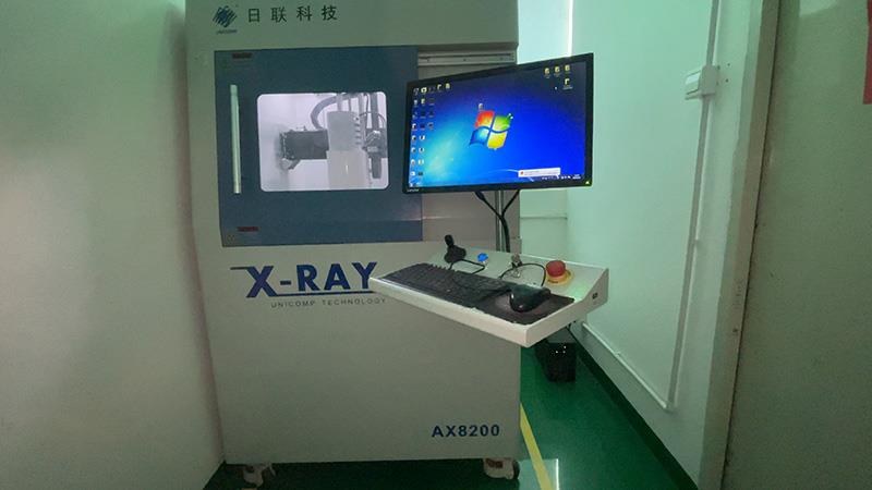
BGA, QFN, and bottom-terminated components cannot be fully inspected by normal visual inspection. Voids, head-in-pillow defects, and insufficient wetting may hide under the package.
These defects are controlled through pad design, paste selection, reflow profiling, and X-ray inspection. If your board uses BGA, LGA, QFN, or power modules with thermal pads, X-ray should be discussed before quotation.
10. PCB Warpage and Mechanical Stress
Warpage can cause poor solder joints, open circuits, component tilt, or assembly difficulty. It is more common on thin boards, large panels, uneven copper distribution, or boards exposed to high reflow temperature.
Good panel design, balanced stack-up, controlled baking, proper fixtures, and correct reflow settings reduce warpage. Avoid very thin PCBs unless the mechanical design truly requires them.
________________________________________
Defect Prevention Starts Before Production
DFM Review
A serious PCBA supplier should review pad design, spacing, solder mask, fiducials, panelization, hole size, component clearance, polarity marking, and test point access.
BOM Verification
BOM quality directly affects assembly quality. Use complete manufacturer part numbers, not vague descriptions. Mark DNI parts clearly. List approved substitutions separately.
First Article Inspection
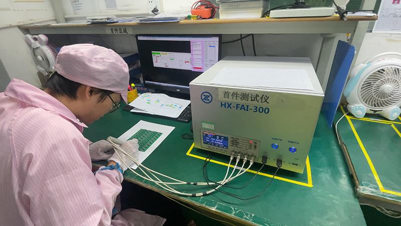
First article inspection confirms that the first assembled board matches the BOM, drawings, polarity, placement, and workmanship standard. It is one of the best ways to prevent batch-level mistakes.
Inspection and Testing Plan
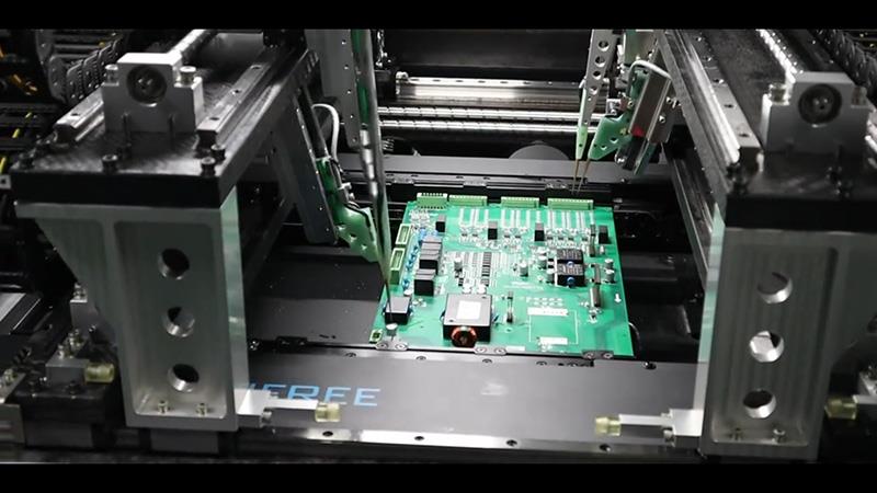
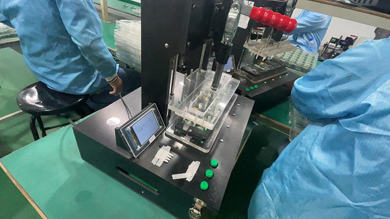
AOI is useful for SMT defects. X-ray is necessary for hidden solder joints. Flying probe test, ICT and functional testing (FCT) verify electrical performance. For higher-reliability products, aging test, conformal coating inspection, or vibration-related review may be needed.
________________________________________
Quick Buyer Reference Table
|
Defect |
Main Risk |
Best Prevention |
|
Solder bridging |
Short circuit |
Stencil control, AOI, DFM review |
|
Insufficient solder |
Intermittent failure |
Paste inspection, clean pads, proper profile |
|
Tombstoning |
Open circuit |
Balanced pad design, stable reflow |
|
Reversed component |
Functional failure |
Clear BOM, polarity drawing, first article check |
|
Poor hole fill |
Weak mechanical joint |
Correct hole size, wave solder control |
|
BGA voids |
Hidden reliability risk |
X-ray, proper pad and reflow design |
|
Flux residue |
Corrosion or leakage |
Process control and cleaning validation |
FAQ: Common Questions About PCB Assembly Defects
Q1: What is the most common PCB assembly defect?
For SMT production, solder bridging, insufficient solder, tombstoning, and component misalignment are common. For through-hole assembly, poor solder filling and reversed manual components are frequent risks.
Q2: Can PCB assembly defects be completely avoided?
No manufacturing process can promise zero risk, but most defects can be reduced through DFM review, controlled materials, first article inspection, AOI, X-ray inspection, and functional testing.
Q3: Should I choose 100% inspection for my PCBA order?
For prototypes, first builds, medical electronics, industrial control boards, or safety-related products, 100% inspection is strongly recommended. For stable bulk production, the inspection plan can be adjusted based on product risk and historical yield.
Q4: What files help reduce assembly defects?
Gerber files, BOM, pick-and-place file, assembly drawing, test procedure, approved component alternatives, and special process notes are the most important. Clear files reduce assumptions.
Q5: Why do prototypes pass but mass production has defects?
Prototype builds often receive more manual attention. Mass production depends more on repeatable process control, panel design, tooling, machine programs, and material consistency. A pilot run is useful before large orders.
Q6: How can overseas buyers control quality remotely?
Use clear documentation, request DFM feedback, approve first article photos or reports, define IPC class requirements, confirm inspection methods, and ask for test records before shipment.
________________________________________
Final Thoughts
Avoiding PCB assembly defects is not only the factory’s responsibility. Buyers, designers, and suppliers must control the project together. Clear files, realistic design rules, correct component selection, stable soldering process, and suitable inspection methods all matter.
For small and medium OEM/ODM buyers, the best strategy is simple: solve manufacturability problems before production starts. This reduces rework, improves yield, protects delivery schedules, and gives your product a stronger path from prototype to bulk PCBA manufacturing.
If you need support with SMT assembly, DIP assembly, hybrid PCBA manufacturing, or defect prevention for a new project, contact us for a customized PCBA quotation and free engineering review.
-
What Is PCBA Functional Testing? A Complete Guide
11 Sep 2026 -

SMT vs Through-Hole Assembly: Which One Should You Choose?
23 Jun 2026 -

What is DFM in PCB Design? A Complete Guide for Exporters & Startups
20 May 2026 -

How to Reduce PCB Manufacturing Cost: 10 Actionable Tips for 2026
09 May 2026 -

PCBA Prototype Service: Fast Turnaround for Product Development
17 Apr 2026 -

How to Ensure Crack-Free PCBs: Inspection, Prevention & Repair
01 Apr 2026