The Role of Chip Mounting in Printed Circuit Boards (PCBs)
 17 Aug 2022 10:27:30 GMT
By admin
Introduction
In the intricate ecosystem of modern electronic devices, printed circuit boards (PCBs) serve as the foundational framework that connects and powers all electronic components. At the heart of this framework lies chip mounting—a critical assembly process that bridges the gap between semiconductor chips and PCBs, enabling the seamless operation of everything from smartphones to industrial machinery. Without precise and reliable chip mounting, even the most advanced electronic designs would fail to deliver their intended performance. This guide explores the essential role of chip mounting in PCBs, the technologies involved, and the impact of this process on electronic device reliability.
What is Chip Mounting?
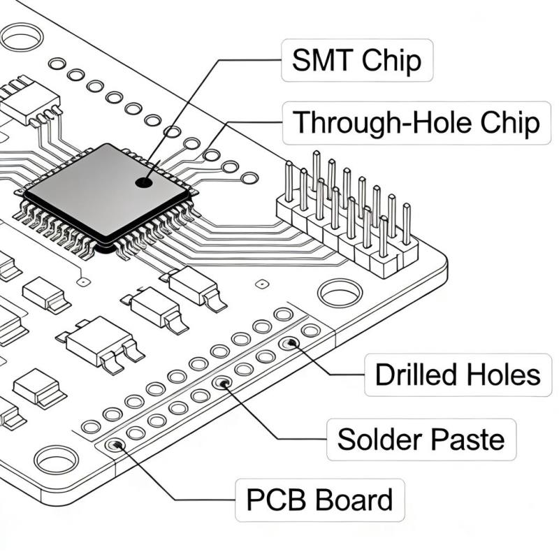
Chip mounting, also known as component mounting, is the process of attaching semiconductor chips and other electronic components to a PCB to establish both electrical connections and mechanical stability. This process is a key step in electronic manufacturing, and its precision directly affects the functionality and lifespan of the final electronic device. There are two primary chip mounting technologies used in modern PCB assembly:

Surface-Mount Technology (SMT)
Surface-mount technology is the most widely used chip mounting method today. In SMT, chips are placed directly onto the surface of the PCB, with their leads soldered to pads on the board. This technology allows for higher component density, smaller device sizes, and faster production speeds compared to traditional through-hole mounting. SMT is ideal for compact electronic devices like smartphones, tablets, and wearable technology, where space is at a premium.
Through-Hole Mounting
Through-hole mounting is a more traditional chip mounting method, where chips with long leads are inserted into pre-drilled holes in the PCB, and the leads are soldered to the opposite side of the board. This method provides greater mechanical stability, making it suitable for components that experience high levels of vibration or physical stress, such as in industrial equipment or automotive electronics. While through-hole mounting is less common in modern compact devices, it remains essential for specialized applications.
Core Roles of Chip Mounting in PCBs
Chip mounting serves five critical functions that are essential to the performance and reliability of electronic devices:
1. Establishing Reliable Electrical Connections
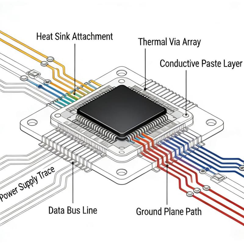
The primary role of chip mounting is to create a stable electrical connection between chips and the PCB. This connection allows electrical signals and power to flow between the chip and other components on the board, enabling the device to perform its intended functions. Precise mounting ensures that each lead of the chip is properly aligned with the corresponding pad on the PCB, preventing open circuits or short circuits that could cause device failure.
2. Providing Mechanical Stability
Chip mounting also provides mechanical stability, securing the chip firmly in place on the PCB. This is essential for ensuring that the chip remains connected even when the device is subjected to physical stress, such as vibration, shock, or temperature changes. Proper mechanical stability prevents the chip from becoming dislodged or damaged, which could lead to intermittent or permanent device failure.
3. Enabling Effective Thermal Management
High-performance chips generate significant amounts of heat during operation, and effective thermal management is essential to prevent overheating and maintain performance. Chip mounting plays a key role in thermal management by creating a path for heat to transfer from the chip to the PCB and eventually to heat sinks or other cooling components. Specialized mounting techniques, such as using thermal paste or conductive adhesive, can enhance heat transfer and improve the overall thermal performance of the device.

4. Ensuring Signal Integrity
In high-speed electronic devices, maintaining signal integrity is critical to prevent signal distortion or loss. Chip mounting affects signal integrity by ensuring that the electrical connections between the chip and PCB are consistent and free from interference. Precise mounting minimizes the length of signal paths and reduces the risk of crosstalk between adjacent signals, ensuring that data is transmitted accurately and efficiently.
5. Optimizing Production Efficiency
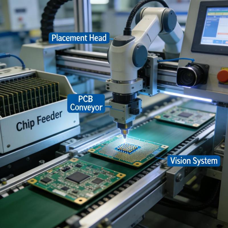
Modern chip mounting processes, particularly SMT, are highly automated, allowing for fast and efficient production of PCBs. Automated mounting equipment can place thousands of chips per hour, significantly reducing production time and costs. This efficiency is essential for meeting the high demand for electronic devices in today's market, while also ensuring consistent quality across large production runs.

Quality Control in Chip Mounting
The quality of chip mounting directly impacts the reliability of electronic devices, and strict quality control measures are essential to ensure that mounting processes meet industry standards. Some key quality control steps include:
• Automated Optical Inspection (AOI): Cameras and image processing technology are used to inspect mounted chips for alignment issues, solder defects, and other problems.
• X-Ray Inspection: For complex components like ball grid array (BGA) chips, X-ray inspection is used to verify the quality of solder joints that are not visible to the naked eye.
• Functional Testing: After mounting, PCBs are tested to ensure that all components are functioning correctly and that electrical connections are stable.
Future Trends in Chip Mounting
As electronic devices continue to become smaller, more powerful, and more complex, chip mounting technology is evolving to meet new challenges. Some key trends in chip mounting include:
• Micro-Mounting Technology: Mounting even smaller chips, such as microelectromechanical systems (MEMS) and nanochips, to enable ultra-compact electronic devices.
• 3D Mounting: Stacking chips vertically on PCBs to increase component density and improve performance in a smaller footprint.
• Smart Mounting Systems: Using artificial intelligence and machine learning to optimize mounting processes, reduce defects, and improve production efficiency.
• Eco-Friendly Mounting: Developing lead-free solders and environmentally friendly mounting materials to reduce the environmental impact of electronic manufacturing.
Conclusion
Chip mounting is a critical process that lies at the heart of electronic device manufacturing, enabling the reliable operation of PCBs and the electronic devices they power. From establishing electrical connections and providing mechanical stability to enabling thermal management and ensuring signal integrity, chip mounting plays an essential role in every aspect of electronic device performance. As technology continues to evolve, chip mounting processes will continue to advance, enabling the development of smaller, more powerful, and more reliable electronic devices. For electronic engineers and manufacturers, understanding the role of chip mounting and investing in high-quality mounting processes is essential to delivering innovative and reliable electronic products to the market.
-
02 Mar 2026 17:51:40 GMT
PCBA Functional Testing: Methods and Industry Standards
-
27 Feb 2026 12:48:42 GMT
The Complete PCBA Quality Control Checklist for Exporters


